
Direct Answer
Testing PCB boards is essential to verify functionality, catch manufacturing defects, and ensure long-term reliability. Whether you're prototyping a new design or scaling to high-volume production, selecting the right combination of test methods—such as ICT, functional test, AOI, and X-ray—depends on board complexity, volume, and risk tolerance.
Omini supports customers across the testing spectrum, helping define test strategies that balance coverage, cost, and turnaround time without over-engineering the validation process.
Why PCB Testing Matters in Manufacturing
Every PCB leaves the assembly line with potential risks: solder bridges, tombstoning, incorrect component orientation, or latent defects from moisture sensitivity or thermal stress. Electrical testing alone won’t catch a solder void under a BGA, and visual inspection might miss a high-impedance intermittent open. That’s why a layered test strategy is critical.
In early production, the goal is to detect assembly defects before they escape to the field. In high-volume runs, the focus shifts to maintaining consistent yield and enabling traceability for process improvement. A well-designed test flow reduces rework, lowers warranty costs, and builds confidence in the final product.
Core Testing Methods for PCBAs
In-Circuit Testing (ICT)
ICT uses a bed-of-nails fixture to make electrical contact with test points on the board. It measures resistance, capacitance, and continuity to detect opens, shorts, missing components, wrong values, and some orientation faults. ICT is fast—often under 30 seconds per board—and ideal for stable, high-volume designs.
Limitations include high fixture cost and inflexibility. If the design changes frequently or volume is low, the fixture investment may not be justified. That’s where alternatives like flying probe come in.
Flying Probe Testing
As discussed in our guide on Demystifying Flying Probe PCB Testing: The What, Why, and How, flying probe uses movable probes to access test points without a fixed fixture. It excels in prototype validation, low-volume production, and design iterations where flexibility outweighs speed.
While slower than ICT, modern flying probe systems have improved throughput and can handle complex analog and mixed-signal measurements. They’re particularly useful for HDI boards with limited test point access.
Functional Testing
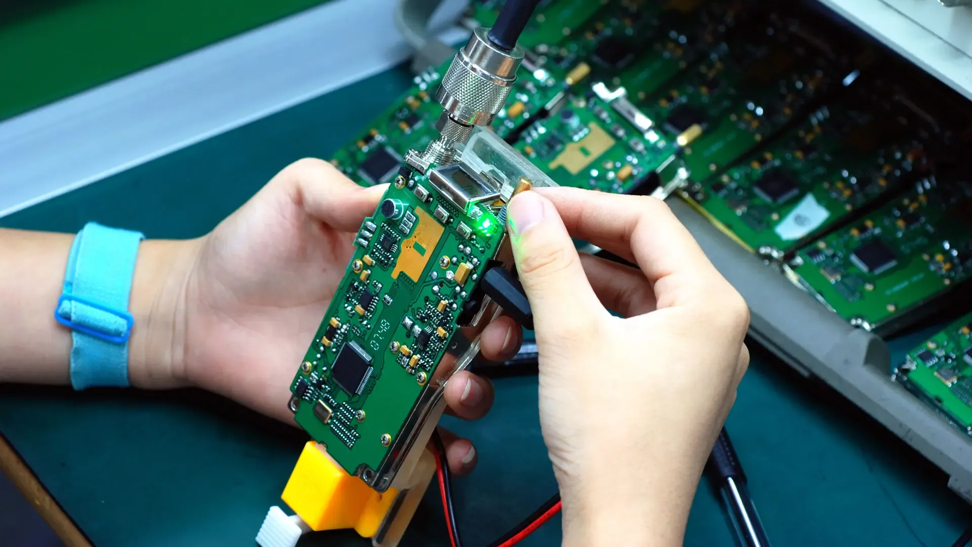
Functional testing powers up the board and applies real-world stimuli to verify it performs its intended function. This might include sending communication signals, checking power regulation, or simulating user interactions. It’s the final gate before shipping but doesn’t diagnose component-level issues.
For example, a board might pass functional test but have a marginal resistor that drifts out of spec under temperature cycling. That’s why functional test should follow, not replace, ICT or flying probe.
AOI and X-Ray Inspection
Automated Optical Inspection (AOI) uses cameras to compare the assembled board against a golden image, detecting solder issues, component misalignment, polarity errors, and missing parts. It’s fast, non-contact, and ideal for post-SMT validation.
X-ray inspection goes deeper, revealing hidden defects like solder voids, insufficient fill, or internal shorts in BGAs and QFNs. As detailed in our article on AOI and X-Ray Inspection in PCB Assembly, X-ray is essential for high-reliability applications where solder joint integrity is critical.
Both AOI and X-ray are preventive—they catch defects before power is applied, reducing false passes in electrical testing.
Building a Test Strategy: From Prototype to Production
Low Volume / Prototyping
For early builds, prioritize flexibility. Use flying probe for electrical validation and AOI for visual checks. X-ray may be reserved for high-risk areas like BGAs or RF modules. Functional testing confirms the design works as intended.
At this stage, Omini often recommends a hybrid approach: flying probe for bring-up, AOI after SMT, and targeted X-ray based on DFM review. This keeps costs low while maintaining visibility into build quality.
Medium Volume
As volumes increase, evaluate the break-even point for ICT fixture investment. If the design is stable and annual volume exceeds a few thousand units, ICT becomes cost-effective. Combine ICT with AOI to catch both electrical and visual defects efficiently.
Consider adding statistical process control (SPC) to monitor test data over time. Trends in ICT failure modes can reveal drift in solder paste viscosity or placement accuracy before yield drops significantly.
High Volume / Mission-Critical
In high-volume or safety-critical applications, redundancy in testing is justified. Use ICT for component-level verification, AOI/X-ray for solder integrity, and functional testing for system-level validation. Implement traceability to link each board’s test results to its component lot, solder paste batch, and reflow profile.
This enables rapid containment if a field issue arises. For example, if a batch of capacitors shows premature failure, traceability can isolate whether the defect originated from a specific supplier lot or reflow oven deviation.
The Role of DFM and Test Point Access
Design for Manufacturability (DFM) directly impacts test effectiveness. During Gerber and BOM review, Omini engineers validate that:
- Sufficient test points are accessible for probe contact
- Components don’t block critical nodes
- Silkscreen markings align with reference designators for visual inspection
- Copper clearances prevent false shorts in ICT
Poor test point access can force reliance on boundary scan or jet printing, increasing test complexity and cost. Addressing these issues early avoids redesigns later.
Traceability and Data Feedback
Modern testing isn’t just pass/fail—it’s a data collection opportunity. By logging ICT results, AOI defect codes, and functional test parameters, manufacturers can build a quality dashboard.
This data supports:
- Root cause analysis after a field return
- Supplier qualification based on component-level test performance
- Process optimization, such as adjusting reflow profiles to reduce solder voids
Omini integrates test data with MES systems to ensure traceability from component receipt to final shipment, supporting audits and continuous improvement.
Common Pitfalls to Avoid
- Skipping AOI to save time: Visual defects often cause electrical failures later.
- Using ICT on unstable designs: Frequent changes make fixture costs unjustifiable.
- Relying solely on functional test: It misses latent defects that escape early failure.
- Ignoring X-ray for BGAs: Assuming solder joints are good based on electrical test risks field failures.
- Over-testing low-volume boards: Flying probe or manual verification may be sufficient.
Practical Field Notes
In production, the best test strategy is the one that fits your actual risk profile—not a checklist from a textbook. Start simple: validate assembly with AOI, verify connectivity with flying probe or ICT, confirm function with functional test, and inspect hidden joints with X-ray where needed.\n As volume grows, let data guide your investments. If ICT repeatedly catches the same resistor misorientation, look at the feeder or placement program—not just the test.
Omini works with engineering teams to tailor test flows that evolve with the product lifecycle, ensuring quality keeps pace with innovation—without slowing it down.
Related Omini Engineering Notes
- Essential Steps for Effective PCB Board Testing
- Circuit Card Assembly Testing: Tips and Best Practice
- PCB Stack-Up and Signal Integrity for High-Speed Boards