
Direct Answer
Planning production capacity for AI server electronics requires accounting for high-layer count PCB fabrication, advanced thermal management via heavy copper, and complex SMT assembly for high-density BGA components. Success depends on synchronizing complex stackup requirements with specialized inspection and reflow profiling to ensure high-reliability performance.
The Complexity of AI Server PCB Fabrication
AI server hardware is fundamentally different from consumer-grade electronics. While a standard consumer board might feature 4 to 8 layers, an AI accelerator or server motherboard often requires 20 to 30+ layers to accommodate high-speed signal routing and power delivery networks (PDN). This complexity directly impacts how you plan fabrication capacity.
When planning, you must consider the material requirements. AI systems demand low-loss laminates to maintain signal integrity at extremely high frequencies. These materials often require different drilling and plating parameters compared to standard FR4. You must also evaluate the Different Production Process Between Heavy Copper PCB and FR4 PCB to ensure the manufacturer can handle the high copper weight needed for high-current power rails without compromising fine-line etching.
Capacity planning for these boards is not just about machine hours; it is about specialized material availability and the precision of the drilling and plating stages. High-layer counts increase the risk of registration errors during lamination, requiring advanced optical alignment technologies during the fabrication process.
Managing Stackup and Material Constraints
The PCB stackup is the foundation of AI server reliability. Because these boards carry massive current densities, the thickness of the copper layers is critical. You must understand How to Calculate Copper Thickness in a PCB: Engineering Guide for Reliability and Cost to ensure the PDN can handle the transient current demands of high-performance GPUs and CPUs without excessive voltage drop.
When planning capacity, remember that thicker copper layers can complicate fine-line etching. If your design requires both high current capacity and extremely fine traces for high-speed signals, the manufacturer's ability to manage these conflicting requirements becomes a bottleneck in the production schedule.
SMT Assembly: The Challenge of High-Density Interconnects
Once the PCB is fabricated, the SMT (Surface Mount Technology) assembly phase begins. For AI servers, the SMT process is significantly more intensive than standard PCBA. The presence of large, high-pin-count BGAs (Ball Grid Arrays) and large thermal pads requires specialized handling.
To understand the full scope of the assembly requirements, you should review Explained: What are the Steps in SMT Assembly Process?. For AI hardware, the stencil design and paste release become critical to ensure that large thermal pads do not cause component tilting or insufficient wetting.
Thermal Management and Reflow Profiling
AI components generate significant heat, requiring large thermal vias and often heavy copper planes. During SMT, this creates a massive thermal mass. A standard reflow profile that works for a small microcontroller will fail on an AI board because the large copper planes act as a heat sink, preventing the solder joints from reaching the required liquidus temperature.
> Manufacturing Rule-of-Thumb: Always request a custom reflow profile for AI-grade boards. The thermal mass of heavy copper and large BGAs necessitates a slower ramp rate and longer soak time to ensure all joints reach the correct temperature without overheating sensitive components.
Capacity planning must account for the extra time required for these specialized profiles. A single high-complexity board may require multiple thermal profiling runs before mass production begins to ensure the process is stable.
Inspection and Quality Assurance for High-Reliability Boards
In AI server electronics, a single solder joint failure can lead to a catastrophic system failure. Therefore, inspection capacity is as important as assembly capacity. Standard AOI (Automated Optical Inspection) is insufficient for the high-density BGA components used in AI accelerators.
Advanced Inspection Requirements
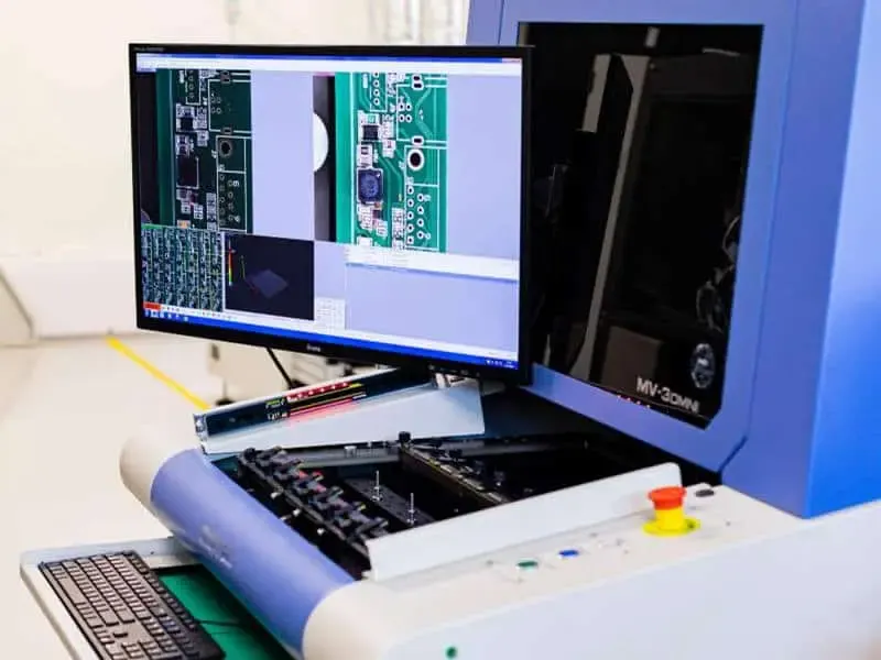
For AI-grade PCBA, 3D X-ray inspection is mandatory to verify the integrity of BGA solder balls under the component. You cannot visually inspect these joints with standard optical methods. When planning production, ensure your partner has the capacity for high-resolution 3D X-ray and can integrate these results into the quality control workflow.
| Inspection Method | Application in AI Servers | Risk if Omitted |
|---|---|---|
| 2D AOI | SMT component placement/polarity | Missing skewed or missing components |
| 3D AOI | Component height and tilt verification | Insufficient solder paste or tilting |
| 3D X-Ray | BGA/LGA solder joint integrity | Hidden voids or shorts under BGA |
| Flying Probe | Electrical continuity and net testing | Open circuits in high-density routing |
Addressing High-Density Interconnect (HDI) Risks
AI servers frequently utilize HDI technology to manage routing density. This often involves microvias, which increase the complexity of the Flex PCB Manufacturing Process: An Overview for Beginners if the design includes flexible interconnects for high-speed signal routing between modules.
Planning for HDI requires ensuring the manufacturer has the capability for laser drilling and copper-filled microvias. These processes are time-intensive and require strict environmental controls to prevent oxidation and contamination.
Common Planning Mistakes and How to Avoid Them
Even experienced engineers can make errors when transitioning from prototyping to high-volume AI server production. Avoiding these mistakes is essential for maintaining a predictable supply chain.
1. Neglecting DFM (Design for Manufacturing) Early in the Cycle
Many engineers treat DFM as a final check before production. For AI servers, DFM must be an iterative process. Issues with trace width/spacing, annular ring size, or copper-to-edge clearances can lead to massive yield losses during fabrication. Always involve your manufacturing partner like Omini during the design phase to review the stackup and SMT requirements.
2. Underestimating Sourcing Lead Times for Critical Components
AI server components—such as high-end FPGAs, GPUs, and specialized memory—often have highly volatile lead times. When planning capacity, you must synchronize the PCB fabrication lead time with the component arrival. A 20-layer PCB might take 4 weeks to fabricate, but if your BGA is on a 26-week lead time, your production line will sit idle.
3. Ignoring Surface Finish and Material Compatibility
The choice of surface finish (e.g., ENIG, ENEPIG, or OSP) is critical for AI servers. ENEPIG is often preferred for high-reliability BGA connections because it provides a flat surface and excellent solderability. However, it is more expensive and requires more processing steps. If you do not specify this clearly in your RFQ, you may face unexpected costs or assembly issues.
4. Overlooking the Complexity of Double-Sided Designs
AI boards are almost always Double Sided PCB: Advantages, Applications, and Manufacturing Process designs to maximize routing density. This doubles the SMT complexity, as each side requires its own stencil, placement, and inspection cycle. Your capacity planning must reflect the total number of SMT passes required for the entire assembly.
Practical Example: Planning a High-Speed AI Accelerator Module
Consider an engineering team designing a new AI accelerator module. The requirements are as follows:
- PCB: 24-layer HDI, high-speed signal layers, heavy copper (3 oz) for power planes.
- Components: Two large BGAs (0.8mm pitch) and several high-speed connectors.
- Assembly: 2-sided SMT, 3D X-ray inspection required.
The Planning Approach:
1. Fabrication Phase: The team must account for the longer lead time for 24-layer HDI fabrication. They must also verify the manufacturer's ability to handle 3 oz copper on signal layers without excessive etching loss. 2. Material Sourcing: The team must secure the low-loss laminates and the BGAs at least 6 months in advance. 3. SMT Phase: The SMT line must be configured for a specific reflow profile that accounts for the high thermal mass of the 24-layer board. The team must schedule time for 3D X-ray inspection for every batch to ensure BGA integrity. 4. Testing Phase: Given the high-speed nature, the capacity plan must include time for high-speed signal integrity testing and functional testing using custom test fixtures.
By following this structured approach, the engineering team avoids the common pitfall of assuming that an AI board can be manufactured using standard consumer-electronics workflows.
Conclusion: Integrating Engineering and Supply Chain
Planning for AI server electronics is a multi-disciplinary challenge that bridges the gap between high-speed electrical design and complex manufacturing logistics. You cannot treat the PCB and the SMT assembly as separate entities; they are deeply interconnected through thermal and mechanical requirements.
To ensure a successful production run, focus on three pillars: rigorous DFM to ensure fabrication yield, specialized thermal management in the SMT process, and advanced inspection to guarantee high-reliability performance. When working with an EMS partner, provide complete technical datasets—including stackups, copper weights, and component coplanarity—to ensure that the capacity planned is the capacity that delivers.
> Engineering handoff note: How to Evaluate Advanced PCB Technology Risk for HDI and Rigid-Flex Projects before the release package is frozen.
> Engineering handoff note: How to Evaluate SMT Assembly Risk from PCB Manufacturing and Sourcing Trends before the release package is frozen.
> Engineering handoff note: How to Evaluate PCB Material Risk from Lamination and Prepreg Trends before the release package is frozen.