
Direkte Antwort
For most standard PCBs, non-conductive epoxy-filled and capped vias are the default choice because they balance cost, reliability, and assembly yield. Choose conductive via fill only when electrical or thermal performance demands it, such as high-current paths or thermal vias. Always specify fill type, plating thickness, and capping requirements in your fabrication notes to prevent DFM rework.
---
The Engineering Principle: Why Via Filling Matters
A via is a plated hole that conducts signals, power, or heat between layers. When left unfilled, the via creates a cavity that can trap air, wick solder during reflow, or provide a path for moisture ingress. The decision to fill a via—and with what material—depends on three engineering variables: electrical requirements, mechanical/thermal loads, and assembly process constraints.
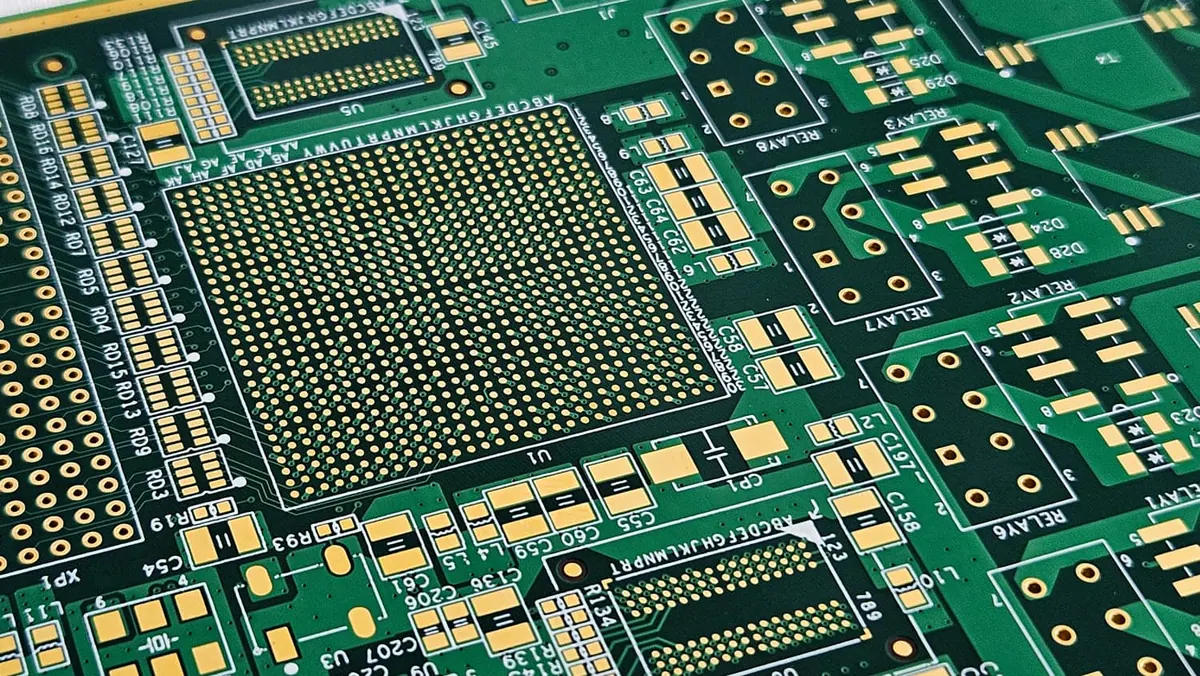
The core principle is that the via fill material must maintain the electrical and thermal integrity of the connection while providing a flat, solderable surface where components are placed. An unfilled via in a BGA pad can cause solder to wick into the hole during reflow, starving the joint of solder and creating voids. This is why via-in-pad designs almost always require filling and capping.
The via aspect ratio—drill diameter divided by board thickness—is the first constraint to check. A 0.2 mm drill through a 1.6 mm board has an aspect ratio of 8:1. Most manufacturers can reliably fill vias with aspect ratios up to 10:1, but beyond that, the fill material may not fully penetrate the hole. This is a manufacturing capability question, not a design rule, so verify it during the DFM review.
---
Non-Conductive Via Fill: The Default Recommendation
Non-conductive via fill uses an epoxy-based material that is vacuum-pressed into the via and then cured. The via is then capped with copper plating, typically 15–25 µm, to create a flat surface. This approach is suitable for most rigid PCB designs, including via-in-pad for BGAs and fine-pitch QFPs.
When Non-Conductive Fill Is the Right Choice
- Standard signal vias that do not carry high current or require low resistance
- Via-in-pad designs for BGA packages where a flat surface is critical for solder joint formation
- Boards with mixed assembly (SMT and through-hole) where solder wicking must be prevented
- Cost-sensitive projects where conductive fill would add unnecessary expense
The epoxy fill material has a coefficient of thermal expansion (CTE) that differs from copper and the laminate. For standard FR4 boards with typical operating temperatures, this is not a concern. However, if the board will see repeated thermal cycling beyond 150°C, discuss the fill material's CTE with your manufacturer.
Capping Requirements
The copper cap over the filled via must be thick enough to withstand the assembly process. A cap that is too thin can crater during component placement or reflow. The cap also needs to be flat—typically within 25 µm of the surrounding pad surface—to ensure consistent solder paste deposition. This flatness requirement is especially critical for fine-pitch components where solder volume is minimal.
> Practical note: For standard via-in-pad designs, specify "epoxy-filled and capped" in your fabrication notes. Do not assume the manufacturer will fill vias by default—many standard processes leave vias unfilled unless explicitly requested.
---
Conductive Via Fill: When Performance Demands It
Conductive via fill replaces epoxy with a conductive material—usually copper or silver-filled epoxy. The filled via provides a continuous conductive path through the hole, which reduces resistance and improves thermal conductivity.
High-Current Applications
For power distribution networks carrying more than 1 A per via, conductive fill reduces the resistance compared to a hollow plated via. A standard plated via with 25 µm copper has a resistance of roughly 0.5 mΩ per mm of depth. Conductive fill can reduce this by 30–50%, depending on the fill material and plating thickness. This matters for boards with high-current motor drivers, power supplies, or battery management systems.
Thermal Management
Thermal vias under power components benefit from conductive fill because the material conducts heat more effectively than air or epoxy. The thermal conductivity of copper is approximately 400 W/m·K, while epoxy is around 0.2–0.5 W/m·K. If you are using vias to conduct heat to an internal copper plane or a heatsink, conductive fill improves the thermal path.
High-Frequency Considerations
In RF designs, a solid copper plug reduces signal distortion by eliminating the impedance discontinuity caused by a hollow via. The via stub effect—where the unused portion of a via acts as a transmission line stub—can be mitigated with back-drilling or conductive fill. For high-frequency designs above 5 GHz, discuss via fill with your manufacturer and consider the material selection guidance in How Do You Select RF PCB Material and the Most Commonly Used Types?
Cost and Process Tradeoffs
Conductive via fill is more expensive than non-conductive fill. The process requires tighter control of plating thickness, and the fill material must be compatible with the surface finish. Silver-filled epoxy can also introduce galvanic corrosion risks if not properly sealed. Reserve conductive fill for designs where electrical or thermal performance justifies the cost.
---
Via-in-Pad: Assembly Yield and Reliability
Via-in-pad is a design technique where vias are placed directly in the component pad. This is common for BGA packages with fine pitch (0.5 mm or less) where routing space is limited. The via must be filled and capped to prevent solder wicking.
Solder Wicking and Voids
During reflow, molten solder can be drawn into an unfilled via by capillary action. This reduces the solder volume at the joint, creating a weak connection or an open circuit. For BGA packages, the solder ball volume is already limited, so any loss to wicking is critical. Filled and capped vias eliminate this failure mode.
Flatness and Coplanarity
The capped via must be flat and coplanar with the pad surface. If the cap is recessed or raised, the solder paste will not deposit uniformly, leading to inconsistent joint heights. This is a common cause of BGA assembly defects that are only detected during electrical test or X-ray inspection.
Design Rules for Via-in-Pad
- Via diameter should be 0.2–0.3 mm for BGA pads with 0.4–0.5 mm pitch
- The cap plating should be at least 15 µm to withstand component placement forces
- The via should be positioned at the center of the pad, not at the edge, to avoid solder mask registration issues
- Verify the via aspect ratio is within the manufacturer's fill capability
---
Manufacturing Constraints and Inspection
Via filling is a process that requires specific equipment and quality control. The manufacturer must vacuum-fill the vias to ensure complete penetration, then cap and planarize the surface. Inspection is performed using cross-sectioning and microsection analysis per IPC-TM-650 test methods.
Aspect Ratio Limits
The maximum aspect ratio for reliable via filling depends on the fill material and process. For epoxy fill, aspect ratios up to 10:1 are typical. Conductive fill may have lower limits due to the viscosity of the material. If your design requires a high aspect ratio, discuss this with the manufacturer during the DFM review.
Plating Thickness Verification
The plating thickness on the via wall and the cap must meet the design requirements. For high-current vias, the plating thickness directly affects resistance and current-carrying capacity. Cross-sectioning is the standard method to verify plating thickness and fill quality. This is part of the qualification requirements under IPC-6012 for rigid PCBs.
Surface Finish Compatibility
The via fill material must be compatible with the surface finish. For example, ENIG (electroless nickel immersion gold) requires a clean, flat surface for the nickel and gold deposition. A poorly planarized via cap can cause surface finish defects. Verify that the fill material and capping process are compatible with your specified surface finish.
---
Common Mistakes That Cause DFM Rework
The following mistakes frequently cause delays and rework during the DFM review. Avoiding them will keep your project on schedule.
Mistake 1: Not Specifying Via Fill Type
Many design files do not include via fill requirements in the fabrication notes. The manufacturer may default to unfilled vias, which can cause assembly issues for via-in-pad designs. Always specify the fill type, material, and capping requirements explicitly.
Mistake 2: Using Conductive Fill Unnecessarily
Conductive fill is expensive and requires tighter process control. Using it for standard signal vias adds cost without benefit. Reserve conductive fill for high-current, thermal, or high-frequency applications.
Mistake 3: Ignoring Aspect Ratio Limits
Designing vias with aspect ratios beyond the manufacturer's capability will result in incomplete fill or voids. Check the aspect ratio during the design phase and adjust the via diameter or board thickness if needed.
Mistake 4: Mixing Fill Types Without Documentation
If a board has both filled and unfilled vias, the design file must clearly indicate which vias require filling. This is often done with a separate drill file or a layer in the CAD data. Without clear documentation, the manufacturer may fill the wrong vias or miss the required ones.
Mistake 5: Not Requesting Cross-Section Verification
Cross-sectioning is the only way to verify fill quality and plating thickness. Request a cross-section report for the first article or during the qualification build. This is especially important for conductive fill, where voids can create hot spots or high-resistance paths.
---
Decision Table for Via Fill Selection
Use the following table as a quick reference during design review. It summarizes the key tradeoffs between fill types.
| Design Condition | Recommended Fill Type | Key Constraint | Inspection Method |
|---|---|---|---|
| Standard signal via, no component placement | Unfilled or tented | Aspect ratio < 10:1 | Visual, AOI |
| Via-in-pad for BGA or QFP | Non-conductive epoxy fill + cap | Flatness within 25 µm | Cross-section, X-ray |
| High-current via (>1 A) | Conductive fill (copper) | Plating thickness ≥ 25 µm | Cross-section, resistance test |
| Thermal via under power component | Conductive fill (copper or silver) | Thermal conductivity | Cross-section, thermal imaging |
| High-frequency via (>5 GHz) | Conductive fill or back-drill | Impedance continuity | TDR, cross-section |
| Mixed assembly (SMT + through-hole) | Non-conductive fill for SMT pads | Solder wicking prevention | X-ray, cross-section |
---
Review Checklist for Fabrication Data
Before sending your design to manufacturing, verify the following items in your fabrication data:
1. Via fill type specified in the fabrication notes for each via class 2. Plating thickness requirement for via walls and caps 3. Capping requirement for via-in-pad designs 4. Aspect ratio of all vias within the manufacturer's capability 5. Surface finish compatibility with the fill material 6. Cross-section request for first article verification 7. Drill file correctly identifies filled vs. unfilled vias
---
Fragen, die Sie Ihrem Hersteller stellen sollten
When you send your design for quote or DFM review, ask these questions to avoid surprises:
- What is the maximum aspect ratio you can reliably fill?
- What is the minimum via diameter for reliable filling?
- What fill materials do you offer (epoxy, copper, silver)?
- Do you perform microsection analysis to verify fill quality?
- What is the additional cost for conductive fill versus non-conductive fill?
- How do you handle via-in-pad designs for fine-pitch components?
These questions are also relevant when selecting a manufacturing partner. The process of evaluating a manufacturer's capabilities is covered in How to Choose a Reliable PCB Manufacturer for Your Project. For boards with mixed material requirements, such as RF and digital sections, also review FR4 vs Rogers PCB Material: Which One Should I Choose for My Products? and the stackup guidance in How to Choose a Suitable 6-Layer PCB Stack-up for Your Projects.
---
Häufig gestellte Fragen
What is the default via hole filling recommendation for a standard PCB?
For most standard rigid PCBs, use non-conductive epoxy-filled and capped vias. This approach provides a flat surface for component placement, prevents solder wicking, and is cost-effective. It is suitable for via-in-pad designs and most BGA packages, provided the via aspect ratio is within the manufacturer's capability.
When should I choose conductive via fill instead of non-conductive fill?
Choose conductive via fill (usually copper or silver epoxy) when you need to carry high current through the via, improve thermal conductivity, or maintain a very low-resistance path. It is also used in high-frequency designs where a solid copper plug reduces signal distortion. Conductive fill is more expensive and requires tighter process control, so reserve it for designs where electrical or thermal performance demands it.
What should I verify in the fabrication data to ensure correct via filling?
Check the fabrication drawing and drill file for via fill type, plating thickness, and capping requirements. Verify that the via aspect ratio is within the manufacturer's capability for filling. Confirm that the via fill material is compatible with your surface finish and assembly process, and request a cross-section report to validate fill and plating quality.
What questions should I ask my PCB manufacturer about via filling?
Ask about the via fill material (epoxy, copper, or silver), the maximum aspect ratio they can fill, and the minimum via diameter for reliable filling. Inquire about their capping process and whether they perform microsection analysis to verify fill quality. Ask about any additional cost or lead time for conductive fill versus non-conductive fill, and how they handle via-in-pad designs.
How does via filling affect assembly yield for BGA and fine-pitch components?
Unfilled vias in pads can cause solder wicking, where solder is drawn into the via during reflow, leading to insufficient solder joints and voids. Filled and capped vias provide a flat, solderable surface, improving wetting and reducing defects. This is especially critical for BGAs and fine-pitch QFPs where solder volume is limited.
What are the common mistakes in via filling that cause DFM rework?
Common mistakes include not specifying via fill type in the fabrication notes, using conductive fill for standard signal vias unnecessarily, ignoring aspect ratio limits, and not requesting cross-section verification. Mixing via fill types on the same board without clear documentation can also lead to process errors and delays.
---
Final DFM Considerations
The via fill decision is part of a broader DFM review that includes material selection, stackup design, and assembly planning. For boards with complex requirements, work with a manufacturing partner early in the design phase. Omini's engineering team can review your via fill specifications and provide feedback on manufacturability before you commit to the design. This collaborative approach is also valuable when selecting a box build partner for complete device assembly, as discussed in How to Choose a Suitable Box Build Assembly Manufacturer for Your Device.
The via fill type affects electrical performance, assembly yield, and long-term reliability. By following the decision framework in this article and verifying your fabrication data against the checklist, you can avoid common pitfalls and ensure your design is manufacturable. Remember that IPC-2221 and IPC-2222 provide the general design framework, IPC-6012 covers rigid PCB qualification, and IPC-TM-650 defines the test methods for verification. Use these standards as references, but always confirm specific capability limits with your manufacturer.
> Engineering handoff note: How to Choose the Best PCB Maker for Your Project before the release package is frozen.
> Engineering handoff note: How to Choose the Right Flexible PCB Material for Your Project before the release package is frozen.
> Engineering handoff note: How to Evaluate PCB Manufacturing Risk from PCB Design and EasyEDA Trends before the release package is frozen.