
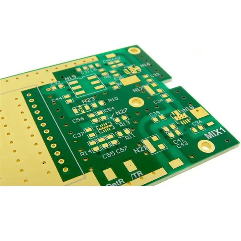
Direct Answer
High-frequency PCB manufacturing requires controlling material electrical properties, copper surface quality, and impedance tolerances through every fabrication step, not just routing accuracy. Engineers must specify laminate Dk/Df, copper weight, surface finish, and test coupons in the RFQ, then verify the manufacturer's process controls for etching, plating, and via hole management to ensure signal integrity above 1 GHz.
Material Selection Drives Electrical Performance
The laminate is the first variable that determines whether a high-frequency PCB will meet its insertion loss and impedance targets. At frequencies above 1 GHz, the dielectric constant (Dk) and dissipation factor (Df) of the base material dominate signal behavior. A stable Dk across frequency and temperature is essential because impedance is inversely proportional to the square root of Dk. If Dk drifts with temperature or moisture absorption, the characteristic impedance shifts, causing reflections and standing waves.
For high-frequency work, common choices include PTFE, hydrocarbon ceramics, and cross-linked PPO (polyphenylene oxide) systems. PTFE offers very low Df but requires specialized drilling and plating processes due to its softness and thermal expansion behavior. Hydrocarbon materials like Rogers RO4000 series provide a balance of low loss and manufacturability. PPO-based laminates are cost-effective but have higher Df, making them suitable only for moderate frequency ranges.
IPC-4101 defines the specification system for laminate materials, including thickness, resin content, and electrical property test methods. When you specify a material grade, reference the IPC-4101 slash sheet that covers it. This ensures the manufacturer sources material that meets the same electrical and mechanical tolerances you used in simulation.
Practical Material Selection Criteria
When comparing laminates, evaluate these properties against your frequency target:
- Dk stability from 1 GHz to your operating frequency
- Df at your operating frequency, not just at 1 MHz
- Moisture absorption rate, which affects Dk in humid environments
- Dimensional stability through lamination and thermal cycling
- Drilling and plating compatibility for your via density
A common mistake is selecting a material based on datasheet values measured at 1 MHz or 10 GHz, then assuming linear behavior between those points. Always request the manufacturer's measured Dk/Df data at your specific frequency band. If the material supplier provides data only at 10 GHz, ask for interpolation guidance or a test coupon measurement.
Stackup Design and Copper Surface Roughness
The stackup defines the impedance of every trace, and the copper surface finish determines how much conductor loss you add on top of the dielectric loss. At high frequencies, current crowds to the surface of the conductor due to the skin effect. Rough copper increases the effective path length and raises resistance, directly increasing insertion loss.
Standard electrodeposited copper foil has a surface roughness of 1.5 to 3 micrometers RMS. For high-frequency work, specify rolled annealed copper or electrodeposited copper with a surface treatment that reduces roughness below 1 micrometer. The etch factor, which is the ratio of etched trace width to the design width, also affects impedance. If the etch removes more copper than expected, the trace becomes narrower, raising impedance above the target.
Stackup Variables to Specify
Your stackup drawing should include:
- Substrate material and grade
- Copper foil weight (e.g., 0.5 oz or 1 oz per square foot)
- Surface roughness target for the copper
- Etch factor tolerance for impedance-critical traces
- Dielectric thickness between layers
- Via type: through, blind, or buried
For a 4-layer design, the internal layer thicknesses and the symmetry of the stackup affect warpage and impedance consistency. Refer to the Manufacturing Process of 4 Layer PCB: Techniques and Best Practices for layer sequencing guidance that applies to high-frequency stackups as well.
> Practical note: Specify copper surface roughness and etch factor in the fabrication notes, not just in the material spec. The plating line and etch process determine the final surface condition, so the manufacturer needs explicit targets to adjust their process.
Impedance Control and Test Coupons
Impedance control is not achieved by simulation alone; it requires physical verification on the fabricated panel. A field solver simulation gives you a theoretical value, but the actual impedance depends on etch factor, copper thickness, dielectric thickness, and surface roughness. These variables have manufacturing tolerances that stack up.
The standard approach is to include impedance test coupons on the PCB panel. These are dedicated traces with known geometry, placed in unused areas of the board. After fabrication, the manufacturer measures the impedance using time-domain reflectometry (TDR) or a vector network analyzer. The measured value is compared against your target and tolerance.
What to Specify for Impedance Testing
- Target impedance value and tolerance (e.g., 50 ohms ± 5%)
- Test coupon location and geometry
- Test method (TDR or VNA)
- Acceptance criteria for the test report
- Number of coupons per panel
A common mistake is specifying impedance tolerance but not defining where the measurement is taken. Impedance varies along a trace due to local stackup variations. Define the measurement point or the average value over the trace length. Also specify whether the test is performed before or after surface finishing, because the plating layer changes the conductor surface and can shift impedance slightly.
Via Stub Management and Signal Integrity
Via stubs are the unused portions of plated through-holes that extend beyond the signal layer. At high frequencies, these stubs act as resonant structures. A stub with a length that is a quarter wavelength at your operating frequency will reflect energy back into the signal path, causing ripple in the passband and increased insertion loss.
The standard mitigation is back-drilling, which removes the stub from the opposite side of the board. Back-drilling adds cost because it requires a secondary drilling operation with precise depth control. If the drill depth is too shallow, the stub remains; if too deep, it damages the signal layer.
Via Design Alternatives
- Blind vias: plated only through the layers that need connection, eliminating the stub entirely
- Buried vias: internal connections that never reach the outer surface
- Back-drilled through vias: standard through holes with the stub removed after plating
Blind and buried vias are preferred for high-frequency designs because they eliminate the stub without an extra process step. However, they require more complex plating processes and may have higher aspect ratio challenges. Discuss via design with the manufacturer during the design for manufacturability (DFM) review. The Decoding High-Density Interconnect (HDI) PCB Technology: An Overview covers via density and aspect ratio considerations that apply to high-frequency boards as well.
Surface Finish Selection for High-Frequency Loss
The final surface finish affects both solderability and high-frequency loss. ENIG (electroless nickel immersion gold) is the most common finish because it provides a flat, solderable surface with good shelf life. However, the nickel layer adds magnetic loss at very high frequencies, typically above 10 GHz. For millimeter-wave applications, the nickel layer can contribute measurable insertion loss.
Immersion silver offers lower loss than ENIG because it does not require a nickel underlayer. The tradeoff is reduced shelf life and higher susceptibility to tarnishing. Immersion tin is another option with low loss but requires careful handling to avoid tin whisker formation.
Finish Selection Criteria
| Finish | Loss at High Frequency | Shelf Life | Handling Complexity |
|---|---|---|---|
| ENIG | Moderate to high | Long | Low |
| Immersion silver | Low | Short | Moderate |
| Immersion tin | Low | Moderate | Moderate |
For frequencies below 10 GHz, ENIG is usually acceptable. Above 10 GHz, evaluate whether the nickel layer is acceptable for your loss budget. If you need the lowest loss, specify immersion silver and plan the assembly schedule to avoid long storage times. Confirm the finish is compatible with your frequency range during the RFQ phase.
Design for Manufacturability Review
A DFM review for high-frequency PCBs must go beyond standard manufacturability checks. The reviewer needs to verify material handling, via stub management, surface finish selection, and impedance test planning. Each of these areas has process implications that affect cost and lead time.
DFM Checklist for High-Frequency Boards
- Confirm the laminate grade is available in the required thickness
- Verify the etch factor tolerance is achievable with the specified copper weight
- Check that impedance test coupons fit in the panel layout without interfering with routing
- Review via types and stub lengths against the operating frequency
- Confirm the surface finish is compatible with the assembly process
- Validate that the stackup is symmetric enough to avoid warpage
A common mistake is treating the DFM review as a purely mechanical check. For high-frequency boards, the electrical properties of the materials and the process tolerances are equally important. The manufacturer needs to know the target impedance, the frequency range, and the acceptable insertion loss to make process decisions.
RFQ Documentation for High-Frequency PCBs
The RFQ is the primary communication tool between the design engineer and the manufacturer. For high-frequency PCBs, the RFQ must include electrical performance requirements that are not typically part of standard PCB quotes.
Required RFQ Information
- Target frequency or frequency band
- Required impedance values and tolerances for each trace group
- Laminate material and grade (e.g., Rogers RO4003C or PTFE)
- Copper weight and surface roughness target
- Surface finish type (ENIG, immersion silver, immersion tin)
- Stackup details including layer thicknesses
- Via types and any back-drilling requirements
- Impedance test coupon requirements
- Special testing such as thermal cycling or insertion loss measurement
The Flex PCB Manufacturing Process: An Overview for Beginners provides a baseline for how process documentation flows from RFQ through fabrication, which applies to rigid high-frequency boards as well. For flexible high-frequency applications, the Introduction to Flex PCBs: Basics and Benefits for Reliable PCBA covers additional reliability considerations.
A clear RFQ reduces the risk of misinterpretation. If the manufacturer does not know the target frequency, they cannot select the correct laminate or surface finish. If the impedance tolerance is not specified, they will use standard process tolerances that may be too loose for your application.
Common Mistakes and How to Avoid Them
Engineers frequently make the same errors when designing high-frequency PCBs. Recognizing these patterns early saves time and cost.
Mistake 1: Ignoring Copper Surface Roughness
The datasheet for the laminate tells you the dielectric loss, but the copper surface roughness determines the conductor loss. Specify the surface roughness target and verify the manufacturer can achieve it with their plating process.
Mistake 2: Not Accounting for the Etch Factor
The etch factor changes the trace width and therefore the impedance. If you design for a 50-ohm trace but the etch removes 0.5 mil more copper than expected, the impedance shifts. Include the etch factor in your impedance calculation and specify the tolerance.
Mistake 3: Forgetting Via Stubs
Via stubs cause resonances that are invisible in a 2D layout review. Always check the 3D model for stub lengths and compare them against the quarter-wavelength at your operating frequency.
Mistake 4: Overlooking Test Coupon Placement
Impedance test coupons are useless if they are placed in a region with different stackup characteristics than the active traces. Place coupons near the critical traces or replicate the same stackup conditions.
Mistake 5: Assuming Standard Surface Finish Is Acceptable
ENIG is the default finish for most PCB manufacturers. If your frequency is above 10 GHz, the nickel layer may add unacceptable loss. Specify the finish explicitly in the RFQ.
When to Involve the Manufacturer
Involve the manufacturer early in the design cycle, ideally during the stackup definition phase. The manufacturer can advise on laminate availability, etch factor capabilities, and via processing constraints before you finalize the design. This is especially important for high-frequency boards where material selection and process tolerances are tightly coupled.
For the DFM review, provide the manufacturer with the target impedance, frequency range, and insertion loss budget. Ask them to confirm their process can meet the etch factor and surface roughness targets. If you need impedance test coupons, confirm they have TDR or VNA capability and can provide a test report.
Omini acts as the manufacturing partner in this workflow, reviewing the stackup, confirming process capabilities, and producing the impedance test report that validates the design. Early involvement reduces the risk of re-spins and ensures the final board meets the electrical requirements.
Verification Before Fabrication
Before releasing the design to fabrication, verify the material properties and impedance requirements are fully specified. Check the laminate datasheet against your frequency range. Confirm the copper weight and surface finish are compatible with the target insertion loss. Review the via design for stub lengths.
Use a field solver to simulate the stackup and trace geometry. Provide the manufacturer with the target impedance values and tolerances. Ask for impedance test coupons on the panel and review the manufacturer's impedance test report after fabrication. Compare the measured values with your simulation results to confirm the process is under control.
If the measured impedance is outside tolerance, work with the manufacturer to identify the root cause. The issue may be the etch factor, copper thickness, or dielectric thickness. Corrective action may involve adjusting the etch process, changing the copper foil weight, or modifying the stackup. Document the corrective action and update the fabrication notes for future builds.
> Engineering handoff note: Exploring Teflon PCBs: A Guide to High-Frequency Applications before the release package is frozen.